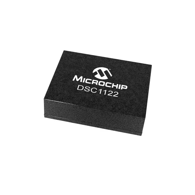
MEMS timing in a 2.5 mm VLGA
The DSC6101JL3B-127K000: The MEMS resonator die is manufactured on a standard CMOS process and hermetically sealed at the wafer level, giving the part inherent resistance to 50,000 g shock and 70 g vibration — relevant for engine-mounted ECUs or transmission controllers.
Maximum supply current is 3 mA typical across the full voltage range and temperature band — at 127 kHz the CMOS output stage draws negligible dynamic current, so the 3 mA figure is dominated by the MEMS PLL and internal regulator bias.
Stability and jitter for the 127 kHz band
For a 127 kHz output, the relevant jitter integration band is typically 10 Hz to 100 kHz (the audio band or a low-speed MCU clock tree). The MEMS oscillator's phase noise is -145 dBc/Hz at 10 kHz offset, giving an integrated RMS jitter well under 1 ps in that band — more than adequate for a UART baud-rate generator or a CAN bus time base. The CMOS output swing is rail-to-rail with a typical rise/fall time of 2 ns into a 15 pF load at 3.3V — the edge rate is fast enough to drive a standard digital input without a Schmitt trigger, but the 127 kHz period (7.87 µs) means the 2 ns edge contributes negligible timing uncertainty.
Lifecycle and compliance posture
Microchip lists this part with AEC-Q100 qualification, meaning the device has passed the full automotive reliability test suite (preconditioning, HAST, temperature cycle, ESD, latch-up) and is PPAP-ready for automotive-tier customers. The MEMS oscillator family shares a common 4-VLGA footprint and pinout across the DSC61XXB frequency range — a 25 MHz variant (DSC6101ME2B-025000) drops into the same PCB land pattern if a higher-frequency reference is needed later, without a board spin.