Active production — what it means for your BOM
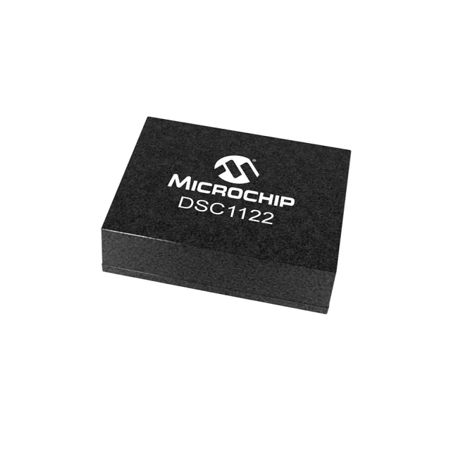
The DSC6021JI2B-01VET: For a board that sees mechanical stress in transit or operation, the MEMS construction eliminates the frequency shift a quartz blank would exhibit under acceleration.
Dual-frequency output and timing budget
This part delivers two independent CMOS clock outputs: 21 MHz and 47 MHz, both from a single MEMS die. For a system that multiplexes two clock domains off one oscillator, the dual-output eliminates a second can and its associated PCB routing. Typical current draw is 1.3 mA max, which keeps the thermal contribution negligible in a dense layout.
The land pattern matches the standard 4-pin VLGA footprint — no custom pad geometry required. The 0.89 mm profile fits under low-clearance shields or in card-edge assemblies where height is constrained.