Power budget and standby behavior
The DSC6011JI2B-040.0000T: Active current draw is 1.3 mA typical at 40 MHz — low enough that the oscillator's contribution to the total power budget is negligible in most systems. The CMOS output swings rail-to-rail, which keeps the rise time short into a standard logic input.
Package and board-fit constraints
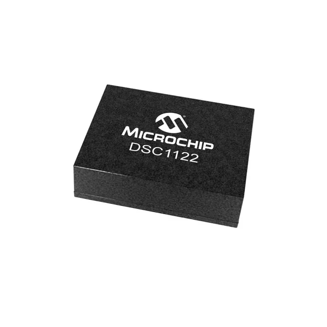
The land pattern is the standard 4-pad VLGA footprint — no thermal pad underneath, so routing the output and supply traces is straightforward on a two-layer board. The 0.89 mm height keeps it under most low-profile enclosure lids. No special bake or moisture sensitivity handling beyond the standard MSL level for a molded plastic package.
Temperature range and deployment context
The ±25 ppm stability holds across this band, so the 40 MHz clock stays within the timing budget for a CAN-FD controller or a high-speed serial interface without external temperature compensation.