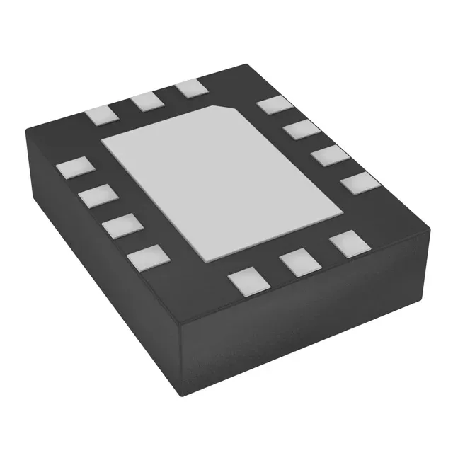
Dual 8 MHz LVPECL clock with wide supply tolerance
The LVPECL differential pair provides low-jitter clock distribution for high-speed ADC/DAC or FPGA reference clocks, but requires proper 50-ohm termination to ground — a common layout gotcha that eats signal integrity if omitted. Its supply voltage spans 2.25 V to 3.6 V, meaning it can run directly off a 2.5 V or 3.3 V rail without an intermediate regulator — one less part on the BOM for mixed-voltage systems.
Frequency stability is ±50 ppm across the full temperature range — tight enough for most 8 MHz reference applications, though a system with a 100BASE-TX PHY that needs ±25 ppm would require a higher-grade sibling in the DSC2222 family.
The 14-VFQFN exposed-pad package (3.20 mm x 2.50 mm, 0.90 mm height) requires a thermal via array under the paddle for proper heat dissipation, especially when sourcing the 89 mA typical supply current.