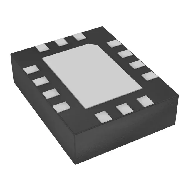
Dual-frequency LVDS clock for tight timing budgets
The LVDS output pairs with high-speed serial interfaces (Gigabit Ethernet, FPGA transceivers, SerDes) where common-mode noise rejection matters.
The package is supplied on tape and reel, ready for automated pick-and-place.
Supply voltage flexibility and LVDS signal integrity
The supply voltage range is 2.25V to 3.6V, covering 2.5V and 3.3V rails commonly found in networking and FPGA boards. The LVDS output swings to a differential voltage that meets the ANSI/TIA/EIA-644 standard, so it can drive a 100-ohm termination directly. The enable/disable function is active-low; pulling the enable pin low tri-states the output, which helps during board-level test or when the downstream device is not ready to receive a clock.