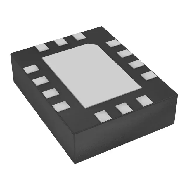
Microchip Technology DSC2044FE2-H0006T — Crystals & Oscillators

DSC2044FE2-H0006T – Microchip MEMS XO, 156.25 MHz HCSL

MPNDSC2044FE2-H0006T
Active

Microchip DSC2044 series MEMS XO (Standard), dual 156.25 MHz HCSL outputs, ±25 ppm stability, 2.25V–3.6V supply, -20°C–70°C, 14-VFQFN exposed pad, tape & reel.

Sourced new & surplus through independent channelsAuthenticity-screened · ESD-safe packingListing updated Aug 2026

Specifications

DSC2044FE2-H0006T specifications
ParameterValue
TypeXO (Standard)
SeriesDSC2044
Voltage2.25V ~ 3.6V
Current - supply60mA (Typ)
Current - supply (Disable)23 mA
Frequency stability±25ppm
Frequency - output 1156.25MHz
Frequency - output 2156.25MHz
Operating temperature-20°C~70°C
Height0.035\" (0.90mm)
Size (Dimension)0.126\" L x 0.098\" W (3.20mm x 2.50mm)
OutputHCSL
PackageTape & Reel (TR)
FunctionEnable/Disable
Base resonatorMEMS
Case14-VFQFN Exposed Pad

Product details

Dual 156.25 MHz HCSL clock source

The DSC2044FE2-H0006T is a MEMS-based XO (Standard) from Microchip's DSC2044 series, delivering two identical 156.25 MHz outputs in HCSL logic levels — the frequency and signal type used as the reference clock for PCI Express Gen 1/2/3 and many 10GbE PHYs. HCSL (High-Speed Current Steering Logic) swings 700–800 mV peak-to-peak into a 50-Ω termination to ground, which means the same output can drive a PCIe slot or a SerDes reference directly without external level translation.

The 2.25V–3.6V supply range lets the oscillator run from a 2.5V or 3.3V rail without a dedicated regulator — useful when the board already carries one of those voltages for the FPGA or switch ASIC. Maximum supply current is 60 mA typical with both outputs active; disabling the outputs via the Enable/Disable pin drops the draw to 23 mA max, which helps meet standby power targets in line-card or access-point designs.

MEMS reliability and temperature range

Package and board layout note

The 14-VFQFN exposed-pad package (3.20 mm x 2.50 mm, 0.90 mm height) requires a thermal pad on the PCB for heat sinking — the pad also provides a low-inductance ground return for the HCSL outputs, which matters for signal integrity at 156.25 MHz.

Frequently asked questions

What is the difference between HCSL and LVDS for this oscillator?

HCSL is a current-mode logic that swings 700–800 mV into a 50-Ω termination to ground, while LVDS swings 350 mV into a 100-Ω differential termination. HCSL is the standard for PCIe reference clocks; LVDS is more common in backplane and SerDes applications. The DSC2044FE2-H0006T outputs HCSL only — if your BOM calls for LVDS, you need a different DSC2044 variant.