Dual 100 MHz HCSL clock source for PCIe reference
The DSC2044FE1-F0022 is a MEMS-based XO (Standard) oscillator delivering two identical 100 MHz HCSL outputs from a single 14-VFQFN package — a dedicated PCIe Gen1/Gen2/Gen3 reference clock generator that eliminates a second oscillator and its associated layout split. The HCSL (High-Speed Current Steering Logic) output swings 0.7 Vpp typical into a 50 Ω termination to ground, matching the differential clock input requirements of Intel PCH, AMD FCH, and most PCIe switch/PHY devices without external level translation. Supply tolerance spans 2.25 V to 3.6 V, so a single BOM line serves both 2.5 V and 3.3 V clock domains — no separate LDO needed when the board has mixed voltage planes.
Package footprint and board layout notes
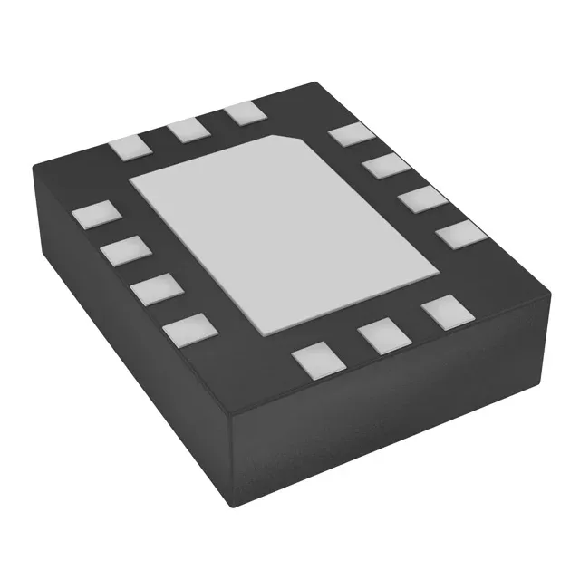
The 14-VFQFN exposed-pad package measures 3.20 mm x 2.50 mm with a 0.90 mm height — the centre pad must be soldered to a ground-plane island with at least four thermal vias to keep junction temperature within the -20°C to 70°C operating range. HCSL outputs require series termination resistors (typically 33 Ω) placed within 0.5 inch of the output pins to control reflections on the 100 Ω differential pair — omit them and the edge rate degrades beyond the PCIe jitter budget.
The base product number DSC2044 covers multiple frequency and stability variants; the -F0022 suffix locks the output frequencies to 100 MHz on both channels with ±50 ppm stability across the -20°C to 70°C range.