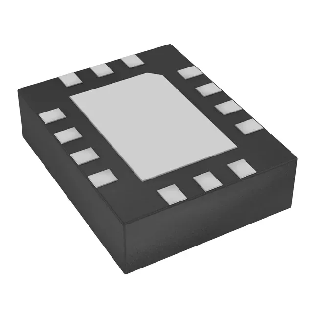
MEMS clock source with dual LVDS outputs
Output 1 covers 100 MHz to 400 MHz; Output 2 spans 25 MHz to 200 MHz — common rates for Ethernet, video, and FPGA reference clocks.
Dual-frequency output flexibility
Two independent frequency banks let a single oscillator serve both a 156.25 MHz Ethernet PHY reference (Output 1) and a 25 MHz system clock (Output 2), reducing the clock-tree component count. The Enable/Disable function on each output allows power gating of unused clock domains, dropping supply current from 38 mA typical to 23 mA max when disabled.
The 14-VFQFN exposed-pad package measures 3.20 mm x 2.50 mm with a 0.90 mm height, fitting tight PCB layouts. Supply voltage ranges from 2.25 V to 3.6 V, covering 2.5 V and 3.3 V rails without an external regulator.