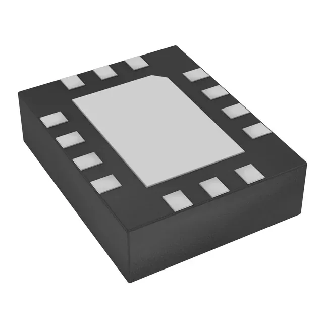
Dual-frequency MEMS XO for clock-tree consolidation
The DSC2033FI2-F0039 is a MEMS-based XO (Standard) from Microchip's DSC2033 series that outputs two independent LVDS clock frequencies: 100 MHz on output 1 and 75 MHz on output 2. This lets a single oscillator feed two clock domains — for example, the 100 MHz reference for a SerDes or FPGA transceiver and the 75 MHz reference for a downstream PLL — without a second can or a clock buffer. The MEMS resonator eliminates the quartz-crystal start-up time and shock sensitivity trade-offs.
Stability and supply tolerance for high-speed links
For a 100 MHz LVDS clock, ±25 ppm translates to a ±2.5 kHz absolute frequency error — well within the capture range of a typical Ethernet PHY or PCIe reference PLL, but tight enough to avoid bit-error accumulation in a long serial frame. The supply voltage range of 2.25 V to 3.6 V covers 2.5 V and 3.3 V rails without an external LDO. The LVDS output common-mode voltage tracks the supply, so the AC-coupling capacitor on the receiver side must be rated for the full 3.6 V rail.
Package and board layout constraints
The 14-VFQFN exposed-pad package measures 3.20 mm x 2.50 mm with a 0.90 mm seated height. The 0.50 mm pitch limits fan-out on two-layer boards; a 4-layer stack-up is the safe choice.