Two 100 MHz LVDS clocks from one MEMS die
Both outputs run at the same frequency — useful when a board needs a clean reference for two SerDes lanes or two FPGAs without splitting a single-ended clock and risking skew.
±25 ppm stability across -40 to +85°C
That budget includes the initial tolerance, temperature drift, and aging — enough margin for a 1 GbE reference clock or a PCIe Gen 1/2 spread-spectrum input without needing a TCXO.
Maximum supply current is 38 mA typical with both outputs active; disable mode drops it to 23 mA.
Microchip lists the DSC2033FI2-F0022T as Active.
14-VFQFN package – board layout notes
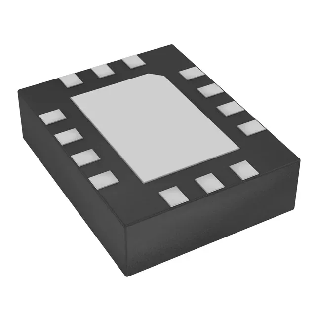
The 14-lead VFQFN with exposed pad measures 3.20 mm × 2.50 mm and stands 0.90 mm off the board.