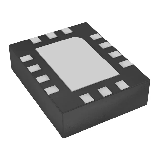
MEMS XO with dual LVDS outputs
This dual-output architecture replaces two separate oscillators, saving board space and reducing BOM count in FPGA or SoC clock trees. The LVDS output provides low-jitter differential signalling suitable for high-speed serial interfaces, with a typical supply current of 38 mA max across the 2.25 V to 3.6 V range.
Industrial temperature and stability
Housed in a 14-VFQFN exposed pad package measuring 3.20 mm x 2.50 mm with a seated height of 0.90 mm, the DSC2033FI1-F0028 requires a thermal pad on the PCB for heat dissipation.