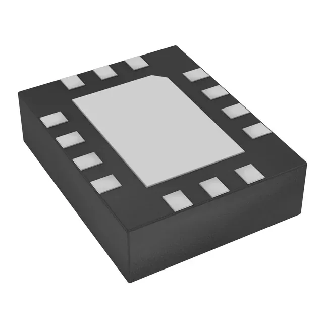
Dual-frequency MEMS XO – 100 MHz and 50 MHz LVDS
The DSC2033FI1-F0025T is a MEMS-based XO (Standard) that generates two independent LVDS clock outputs from a single resonator: 100 MHz on output 1 and 50 MHz on output 2. This eliminates a second oscillator footprint and the associated routing for a common dual-clock scenario — FPGA core logic at 100 MHz and a 50 MHz reference for the PHY or transceiver. Supply voltage spans 2.25 V to 3.6 V, covering 2.5 V and 3.3 V rails without an external regulator.
Industrial temperature and stability for timing-critical boards
For a 100 MHz clock, that is a maximum drift of ±5 kHz — well within the capture range of a typical Ethernet PHY or SerDes PLL. The 38 mA typical supply current is modest, but the pad still needs a solid ground connection to keep the die temperature within spec in a still-air enclosure.
Microchip lists the DSC2033FI1-F0025T as Active.