Dual-output MEMS oscillator for tight-timing boards
Output frequencies land in the 24.99875–25.0025 MHz band, covering common 25 MHz references for Ethernet PHYs, USB hubs, and FPGA transceiver banks. The ±25 ppm frequency stability across -40°C to 85°C keeps the timing budget tight enough for 100BASE-TX and USB 2.0 without a TCXO. Supply voltage spans 2.25V to 3.6V — it runs off a 2.5V or 3.3V rail directly, no extra regulator. The Enable/Disable function lets firmware gate the second output to save power when the peripheral is idle.
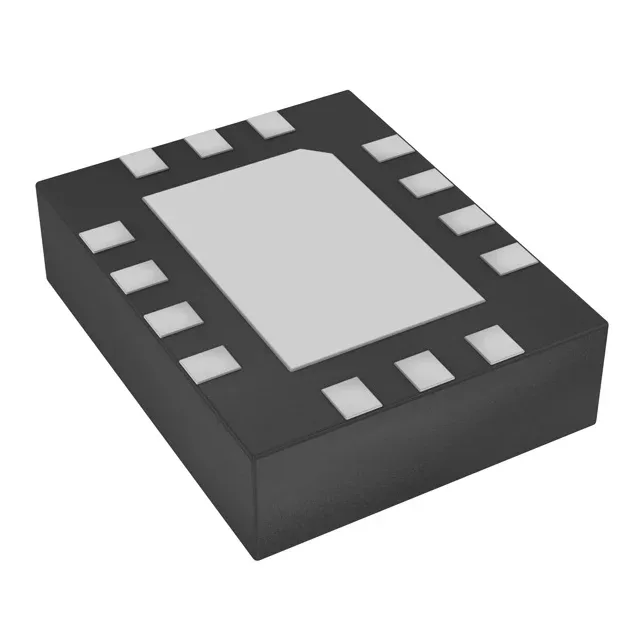
The 14-VFQFN Exposed Pad package measures 3.20 mm x 2.50 mm with a 0.90 mm height — compact enough for a space-constrained NIC or IoT gateway. The exposed pad under the part needs a thermal via array to the ground plane; without it the junction temperature rises above the 85°C ambient ceiling. The CMOS output swing is rail-to-rail, so the trace impedance to the load should stay under 50 Ω to avoid ringing on fast edges.
The base product number DSC2011 covers multiple frequency and stability variants. If the exact output frequency pair or ppm grade changes, a different suffix in the same package footprint keeps the board layout unchanged.