Microchip Technology DSC2010FI2-A0024 — Crystals & Oscillators

DSC2010FI2-A0024 MEMS XO – 26.973 MHz & 27 MHz, LVCMOS

MPNDSC2010FI2-A0024
Active

Microchip DSC2010FI2-A0024, MEMS-based XO (Standard), dual-output 26.973 MHz & 27 MHz LVCMOS, ±25 ppm stability, 2.25–3.6 V supply, -40 to +85 °C, 14-VFQFN exposed pad

Sourced new & surplus through independent channelsAuthenticity-screened · ESD-safe packingListing updated Aug 2026

Specifications

DSC2010FI2-A0024 specifications
ParameterValue
TypeXO (Standard)
SeriesDSC2010
Voltage2.25V ~ 3.6V
Current - supply35mA
Current - supply (Disable)23 mA
Frequency stability±25ppm
Frequency - output 126.973MHz, 27MHz
Operating temperature-40°C~85°C
Height0.035\" (0.90mm)
Size (Dimension)0.126\" L x 0.098\" W (3.20mm x 2.50mm)
OutputLVCMOS
PackageTube
FunctionEnable/Disable
Base resonatorMEMS
Case14-VFQFN Exposed Pad

Product details

Dual-frequency MEMS XO for tight-timing BOMs

The DSC2010FI2-A0024: This MEMS-based XO (Standard) generates two independent LVCMOS clock outputs: 26.973 MHz and 27 MHz, both with ±25 ppm frequency stability over the -40 to +85 °C industrial range.

14-VFQFN exposed-pad mounting and thermal interface

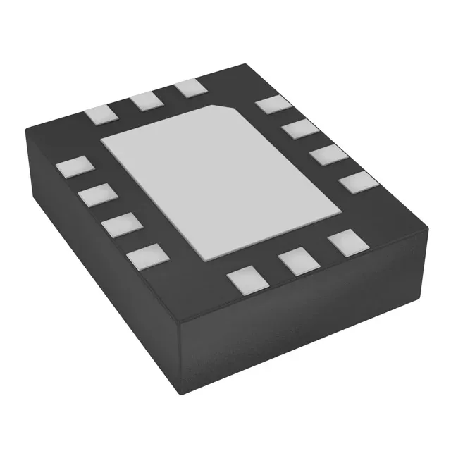
The 14-VFQFN Exposed Pad package measures 3.20 mm x 2.50 mm with a 0.90 mm seated height — the exposed paddle must be soldered to a PCB thermal land to achieve the rated thermal impedance and to provide a low-inductance ground return for the MEMS core. The QFN package demands a solder-paste stencil aperture that matches the pad geometry; a via-in-pad array under the paddle improves heat spreading when the oscillator sits near a hot FPGA or PHY.

Frequently asked questions

What are the exact output frequencies of the DSC2010FI2-A0024?

The DSC2010FI2-A0024 outputs two LVCMOS clocks: 26.973 MHz and 27 MHz. Both frequencies are generated from the same MEMS resonator and are available simultaneously on separate output pins.

Does the DSC2010FI2-A0024 have an enable/disable function?

Yes, the Enable/Disable pin controls the output. When disabled, the supply current drops to a maximum of 23 mA compared to 35 mA when active, allowing the system to save power when the clocked device is in sleep mode.