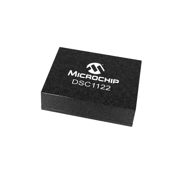
This eliminates the quartz cold-start jitter and the mechanical shock sensitivity that can cause frequency shifts in high-vibration environments — a common failure mode in industrial and outdoor telecom gear. The output is LVCMOS at 25 MHz, a standard logic level that drives most MCU and FPGA clock inputs directly without external level translation.
Supply rail and temperature grade — fit check for the design
The oscillator operates from a 1.8V supply. This is the core voltage for many low-power FPGAs and MCUs — confirm the clock input bank on your device accepts 1.8V LVCMOS before committing the BOM.
Package and footprint — 4-VFLGA layout notes
The 4-VFLGA package measures 2.00mm x 1.60mm with a seated height of 0.89mm. The LGA footprint requires a solder-paste stencil with aperture matching the land pattern — the pad openings should be slightly smaller than the package pads to avoid bridging. No via-in-pad is needed; the four terminals are peripheral.