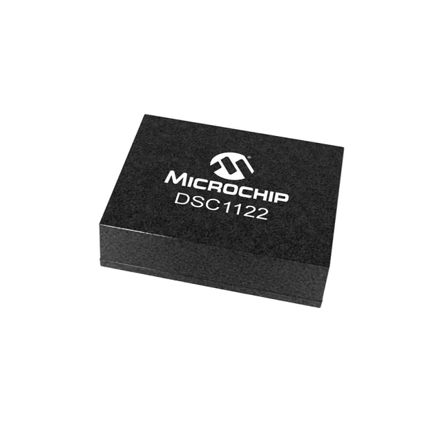
The DSC1522AA3A-25M00000: Frequency stability is held to ±20 ppm across that entire temperature range, tighter than the ±50 ppm or ±100 ppm common on basic crystal oscillators — important for timing-sensitive interfaces like USB full-speed or 100BASE-TX where clock jitter directly affects link margin.
Supply voltage and output compatibility
Supply voltage range spans 2.5V to 3.3V, letting it run from a 3.3V or 2.5V rail without a separate LDO — useful when the same BOM runs on both 3.3V and 2.5V logic domains. LVCMOS output is the standard single-ended clock interface for most MCUs, FPGAs, and SoCs — no level translation or AC-coupling needed for a typical 3.3V or 2.5V logic input.
Package and PCB layout note
The 4-pin footprint is straightforward to hand-solder or reflow; the exposed pad is the only thermal challenge — a stencil aperture covering 50-70% of the pad area prevents solder voids.
Current consumption and power budget
Maximum supply current is 7.5 mA — low enough for battery-operated equipment or thermally constrained designs; at 3.3V that's under 25 mW, negligible in a multi-rail system.