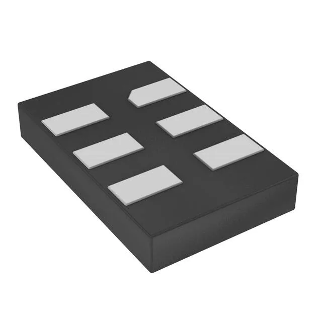
100 MHz HCSL reference clock — MEMS construction
The HCSL output is designed for high-speed differential clock distribution — common in PCIe reference clocks, Ethernet PHY reference inputs, and FPGA clock trees that expect a current-mode differential signal.
The supply voltage spans 2.25V to 3.6V, covering both 2.5V and 3.3V rails without an external LDO.
Enable/Disable function and package outline
The 6-SMD, No Lead package measures 5.00 mm x 3.20 mm with a seated height of 0.90 mm — a standard 5×3.2 mm oscillator footprint that fits many existing PCB layouts designed for quartz oscillators of the same size.