100 MHz HCSL clock for PCIe reference
This frequency and logic family directly serve as the PCIe Gen1/Gen2/Gen3 reference clock — the 100 MHz HCSL signal drives the differential clock pair on the add-in card or motherboard without an external translator.
Operates from 2.25V to 3.6V, covering both 2.5V and 3.3V rails — a single BOM line works across mixed-voltage systems without a regulator swap.
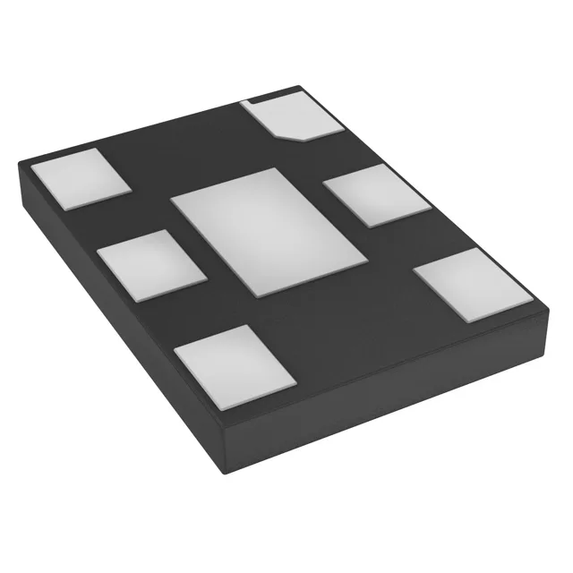
Housed in a 6-SMD, no-lead exposed-pad package measuring 7.00mm x 5.00mm with a seated height of 0.90mm. The HCSL outputs require external series termination resistors (50 Ω to ground at each output) to set the differential swing; the termination is not integrated.
Listed as Active by Microchip.