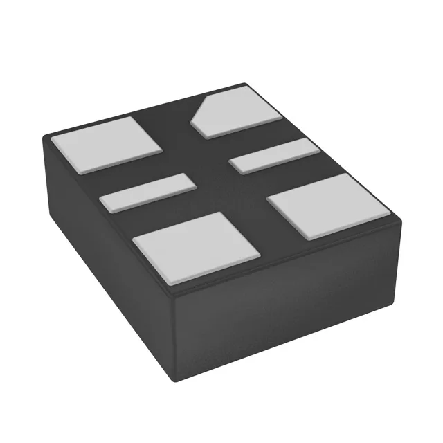
The LVDS output delivers the differential swing needed for high-speed serial interfaces — Ethernet PHY reference clocks, FPGA transceiver banks, or SerDes framers — without the common-mode noise coupling that plagues single-ended clock distribution in mixed-signal boards. It suits engine-control ECU clock trees, ADAS camera serialiser reference clocks, and body-domain CAN-FD controllers where the ambient under the dashboard or behind the headlamp module exceeds 85°C.
Supply range, enable function, and current budget
The supply voltage spans 2.25 V to 3.63 V, covering the common 2.5 V and 3.3 V rails without an external LDO. For a 125 MHz carrier, that is a maximum deviation of ±3.125 kHz — tight enough for most 1000BASE-T Ethernet and PCIe Gen 1 reference clock jitter budgets without external VCXO trimming.