For a design targeting under-hood or chassis-domain deployment, this qualification removes the need for a separate PPAP waiver or customer-specific reliability sign-off.
Supply voltage tolerance — one oscillator, three logic families
The DSC1123DI5-100.0000 operates over a 2.25V to 3.63V supply range, covering 1.8V, 2.5V, and 3.3V nominal rails without an external LDO or level translator. This simplifies the BOM when the same oscillator feeds an FPGA bank at 2.5V and a SerDes at 3.3V — the supply pin just follows the rail.
Frequency stability and output drive — what ±10 ppm and LVDS mean for the clock tree
For a 1 Gbps SerDes link, that keeps the recovered clock within the CDR tracking bandwidth without bit-error-rate degradation. LVDS output delivers a 350 mV swing into a 100 Ω differential termination, which is the standard interface for clocking high-speed ADCs, FPGAs, and SerDes devices. The 32 mA max supply current covers the output driver and the MEMS PLL — well within the budget of a 3.3V rail.
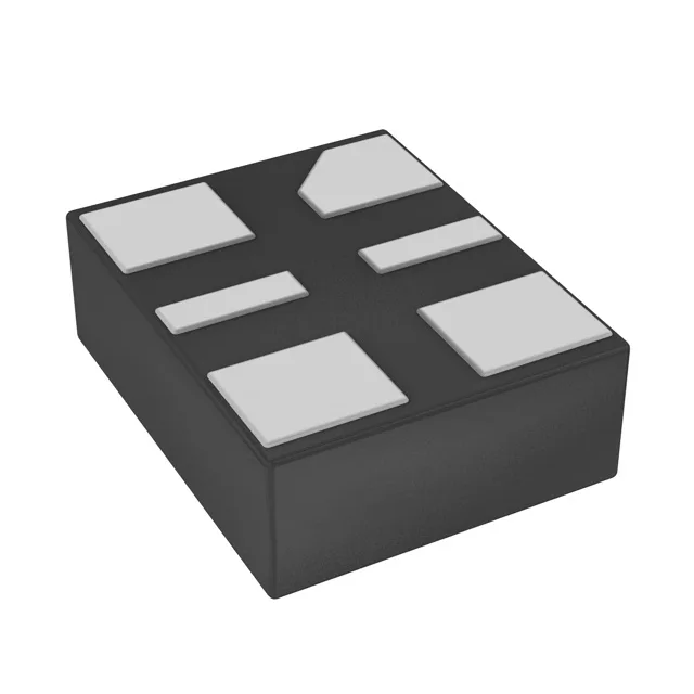
The 6-SMD no-lead package, 0.098" x 0.079" (2.50 mm x 2.00 mm) with a 0.90 mm seated height, fits the same land pattern as many 2.5 x 2.0 mm quartz oscillators — but the MEMS die eliminates the need for a separate quartz blank and allows the same PCB layout to serve multiple frequency variants from the DSC1123 family.