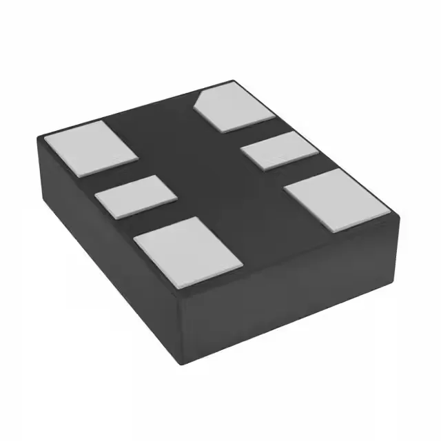
125 MHz LVDS clock source with automotive-grade qualification
The LVDS output delivers the low-jitter, differential signal required for high-speed SerDes, FPGA reference clocks, and Ethernet PHY timing.
The supply voltage range of 2.25V to 3.63V lets this oscillator run directly from a 2.5V or 3.3V rail — no dedicated LDO needed. That disable current matters for sleep-mode power budgets in battery-backed or ignition-off automotive modules.
Housed in a 6-SMD, no-lead package measuring 3.20mm x 2.50mm with a seated height of 0.90mm. The 0.50 mm pitch land pattern is standard for this footprint class — route the differential LVDS pair with controlled impedance (50 Ω single-ended, 100 Ω differential) and keep the supply decoupling within 2 mm of the VDD pin.