The LVDS differential output delivers low-jitter clocking for high-speed serial interfaces (CAN-FD, Ethernet, SerDes) where single-ended CMOS noise coupling becomes a signal-integrity risk. Supply voltage spans 2.25V to 3.63V, covering both 2.5V and 3.3V rails without an external LDO — a single rail feeds the oscillator, simplifying the power tree on a mixed-voltage ECU board.
Package footprint and reflow considerations
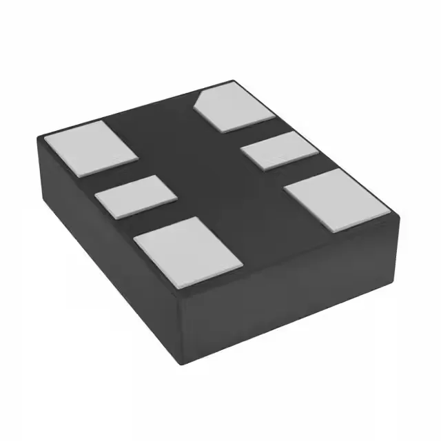
Housed in a 6-SMD, no-lead package measuring 2.50mm x 2.00mm with a seated height of 0.90mm. The 0.50mm pitch land pattern demands a solder-paste stencil aperture sized to avoid bridging between the LVDS output and supply pads. The Enable/Disable pin (pad 1) lets the system power-gate the oscillator: when pulled low, the output goes high-impedance and supply current drops from 32 mA to 22 mA max. This is useful for sleep-mode current budgets in battery-backed automotive modules.