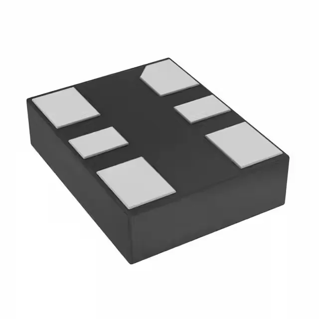
Microchip Technology DSC1123CI2-333.3333T — Crystals & Oscillators

DSC1123CI2-333.3333T MEMS XO, LVDS 333.3333 MHz, Active

MPNDSC1123CI2-333.3333T
Active

Microchip DSC1123 series MEMS XO, 333.3333 MHz LVDS output, ±25 ppm stability, 2.25V–3.63V supply, -40°C to 85°C, 6-SMD package, Enable/Disable function.

$3.3000Ref. price · indicative, final on quote
Independent supplier — new & surplus stockAuthenticity-screened · ESD-safe packingListing updated Aug 2026

Specifications

DSC1123CI2-333.3333T specifications
ParameterValue
TypeXO (Standard)
SeriesDSC1123
MountingSurface Mount
Supply voltage2.25V ~ 3.63V
Current - supply32mA
Current - supply (Disable)22mA
Frequency333.3333 MHz
Frequency stability±25ppm
Operating temperature-40°C~85°C
Size (Dimension)0.126\" L x 0.098\" W (3.20mm x 2.50mm)
Height - seated0.035\" (0.90mm)
OutputLVDS
PackageTape & Reel (TR)
FunctionEnable/Disable
Base resonatorMEMS
Case6-SMD, No Lead

Product details

333.3333 MHz LVDS clock — what it buys the design

The DSC1123CI2-333.3333T delivers a 333.3333 MHz LVDS output from a MEMS resonator, not a quartz crystal — no start-up time, no crystal load-cap selection, and no frequency-pulling from board parasitics. The LVDS differential pair keeps the signal clean over a short PCB trace to the FPGA or SerDes reference input.

Supply rail and power budget

The supply range spans 2.25V to 3.63V, so it runs from a 2.5V or 3.3V rail without an intermediate LDO.

6-SMD, no-lead package, 3.20 mm x 2.50 mm body, 0.90 mm seated height. The MEMS die is inside the package; no external crystal or load capacitors are needed.

Frequently asked questions

Does DSC1123CI2-333.3333T have a pin-compatible alternative in the DSC1123 family?

The DSC1123 series shares the same 6-SMD footprint and supply range across frequency variants. A different frequency (e.g., 312.5 MHz or 400 MHz) would be a different order code but the same pinout — confirm the exact frequency your PLL or FPGA reference requires before substituting.

What is the output type and what does it drive?

LVDS differential output, 333.3333 MHz. It drives a 100-ohm differential termination at the receiver — typical for FPGA clock inputs, SerDes reference clocks, or high-speed ADC/DAC sample clocks. The Enable/Disable pin lets the output be tri-stated for test or power saving.