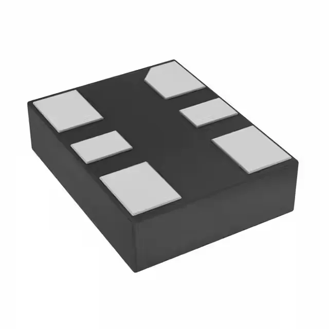
180 MHz LVDS clock source for harsh environments
Supply voltage and output control
Operates from a single 2.25V to 3.63V supply, covering 2.5V and 3.3V logic rails without an external regulator — the Enable/Disable function lets the system gate the clock output, pulling the disable current down to 22 mA max. The LVDS output pairs directly with high-speed SERDES, FPGA clock inputs, or Ethernet PHY reference clocks — the differential signalling keeps noise coupling low on a mixed-signal board.
Housed in a 6-SMD, no-lead package measuring 3.20mm x 2.50mm with a seated height of 0.90mm — the compact footprint fits tight layout zones near the processor or FPGA without blocking fan-out vias.