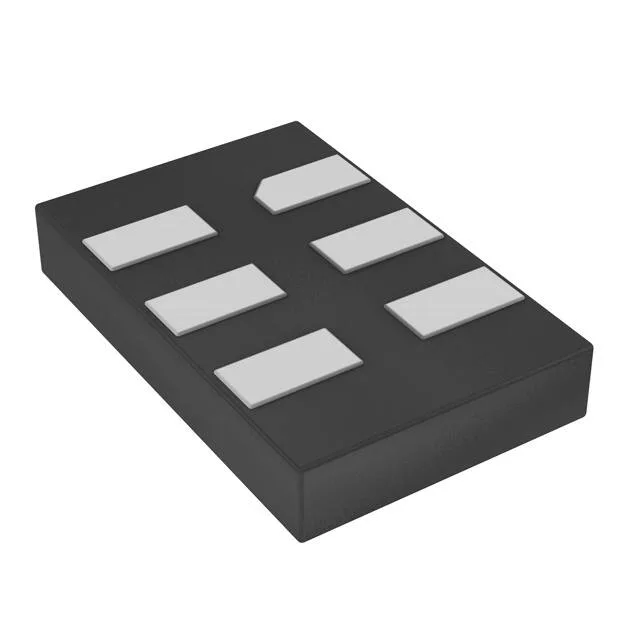
125 MHz LVDS clock with automotive-grade qualification
The DSC1123BI1-125.0000T: The LVDS differential pair keeps jitter low and common-mode noise rejection high, making this oscillator suitable for clocking high-speed ADCs, FPGAs, or serial links in a noisy environment.
Supply rail and enable/disable control
Operates from a 2.25V to 3.63V supply, which covers 2.5V and 3.3V logic rails with margin for both ends. That 10 mA saving matters in a battery-backed or thermally constrained assembly.
Housed in a 6-SMD, no-lead package measuring 5.00 mm x 3.20 mm with a seated height of 0.90 mm. The 0.197" x 0.126" footprint is common across the DSC1123 family, so a single PCB layout can serve multiple frequency variants. Surface-mount assembly follows standard reflow profiles for lead-free solder; no special bake-out or moisture sensitivity label is required beyond the standard MSL 1 typical of MEMS oscillators.
No pin-compatible second source is cited, but the MEMS oscillator market has functional equivalents from SiTime and others that can be evaluated for a second-source BOM slot.