The LVDS signalling provides low-jitter differential clocking for high-speed serial interfaces such as PCIe, SATA, or 10GbE PHY reference clocks, where single-ended CMOS would introduce common-mode noise.
The supply voltage range of 2.25 V to 3.63 V covers common 2.5 V and 3.3 V rails, so no extra regulator is needed when the oscillator shares a rail with the downstream LVDS receiver.
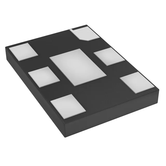
Housed in a 6-SMD, No Lead Exposed Pad package measuring 7.00 mm x 5.00 mm with a seated height of 0.90 mm, the footprint matches industry-standard 7x5 mm oscillator pads.