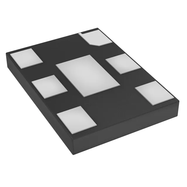
The DSC1123AI5-148.5000: The LVDS output is a differential pair, giving better noise immunity than single-ended CMOS at high frequencies—critical for clean clock distribution in automotive camera, radar, or infotainment links where signal integrity matters.
The -40 to 85°C operating range suits cabin, body, and chassis domains; for under-hood engine-bay locations requiring 125°C, verify a grade-0 variant in the DSC1123 family.
Package, supply, and board-fit notes
Housed in a 6-SMD, No Lead Exposed Pad package, 7.00 x 5.00 mm, 0.90 mm seated height—a standard footprint that drops into existing LVDS oscillator pads without a respin. Supply voltage range 2.25V to 3.63V covers common 2.5V and 3.3V rails, with a max supply current of 32 mA (22 mA when disabled).