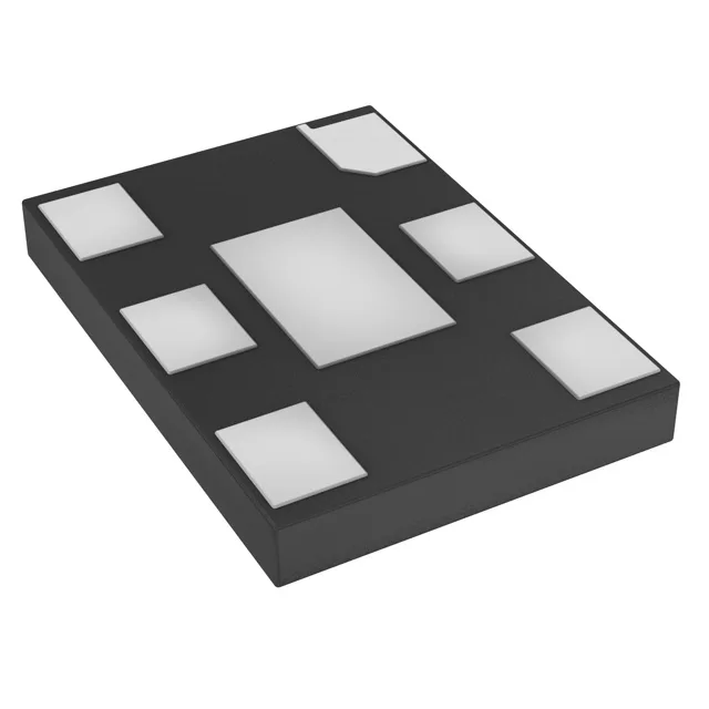
110 MHz LVDS clock source with MEMS resonator
Output is LVDS, which means the differential swing stays within 350 mV typical into a 100-Ω termination — the low swing reduces radiated EMI compared to a single-ended CMOS clock at the same frequency, a real advantage when routing the 110 MHz reference across a multi-layer board near RF or sensor traces.
Rated AEC-Q100 and specified over -40 to 85°C, this oscillator is qualified for automotive under-hood and cabin electronics — an ECU, ADAS camera module, or gateway that sees 85°C ambient on a summer day still holds the ±10 ppm stability window. The ±10 ppm figure includes initial tolerance, temperature drift, and supply variation — no external trim capacitors or calibration step needed at board assembly.
Supply range and disable function
Supply voltage spans 2.25 V to 3.63 V, covering the common 2.5 V and 3.3 V rails without a separate LDO — the internal regulator rejects supply ripple down to the noise floor of the LVDS output.