That 156.25 MHz frequency is a common reference for 10 Gigabit Ethernet, PCIe Gen 3, and FPGA transceiver clocks — the LVDS differential pair keeps jitter low over the trace run to the PHY or FPGA bank. Supply voltage spans 2.25V to 3.63V, so the same part works on a 2.5V or 3.3V rail without a dedicated LDO — the Enable/Disable pin pulls the output to high-Z and drops supply current from 32 mA to 22 mA max for power gating.
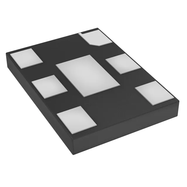
DSC1123AI2-156.2500T – Microchip MEMS LVDS Oscillator
MPNDSC1123AI2-156.2500T
Active
Microchip Technology DSC1123 series, XO (Standard), LVDS output, 156.25 MHz, MEMS resonator, 6-SMD no-lead exposed pad, -40°C to +85°C, AEC-Q100 qualified.
$5.1800Ref. price · indicative, final on quote
Independent supplier — new & surplus stockAuthenticity-screened · ESD-safe packingListing updated Aug 2026
Specifications
| Parameter | Value |
|---|---|
| Type | XO (Standard) |
| Series | DSC1123 |
| Mounting | Surface Mount |
| Supply voltage | 2.25V ~ 3.63V |
| Current - supply | 32mA |
| Current - supply (Disable) | 22mA |
| Frequency | 156.25 MHz |
| Frequency stability | ±25ppm |
| Operating temperature | -40°C ~ 85°C |
| Size (Dimension) | 0.276\" L x 0.197\" W (7.00mm x 5.00mm) |
| Height - seated | 0.035\" (0.90mm) |
| Output | LVDS |
| Package | Tape & Reel (TR) |
| Ratings | AEC-Q100 |
| Function | Enable/Disable |
| Base resonator | MEMS |
| Case | 6-SMD, No Lead Exposed Pad |
Product details
Frequently asked questions
What is the output type of the DSC1123AI2-156.2500T?
LVDS differential output. The 156.25 MHz LVDS signal is compatible with most FPGA clock inputs, Ethernet PHY reference pins, and SerDes reference clocks that expect a 100-ohm differential termination.
Is the DSC1123AI2-156.2500T AEC-Q100 qualified?
This qualifies it for automotive applications including engine control units, ADAS cameras, and infotainment modules that require the extended reliability stress of the AEC-Q100 program.