The Enable/Disable function tri-states the output, reducing supply current from 32 mA to 22 mA when disabled.
The supply voltage range of 2.25V to 3.63V covers both 2.5V and 3.3V rails without an external LDO. The LVDS output is DC-coupled to the receiver, so the common-mode voltage is set by the supply; at 3.3V the output differential swing is about 350 mV typical, compatible with standard LVDS inputs. A 62.5 MHz LVDS clock is a common reference for Ethernet PHYs, FPGAs, and SoCs requiring low-jitter differential timing. The ±25 ppm stability keeps the accumulated timing error within one UI over typical cable or PCB trace lengths at this frequency.
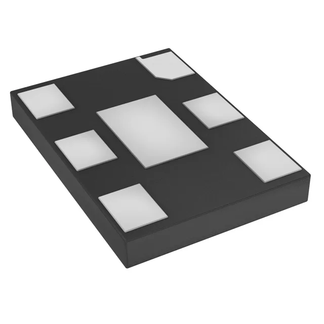
Housed in a 6-SMD, No Lead Exposed Pad package measuring 7.00mm x 5.00mm with a seated height of 0.90mm, the footprint matches industry-standard 7x5 mm oscillator pads.