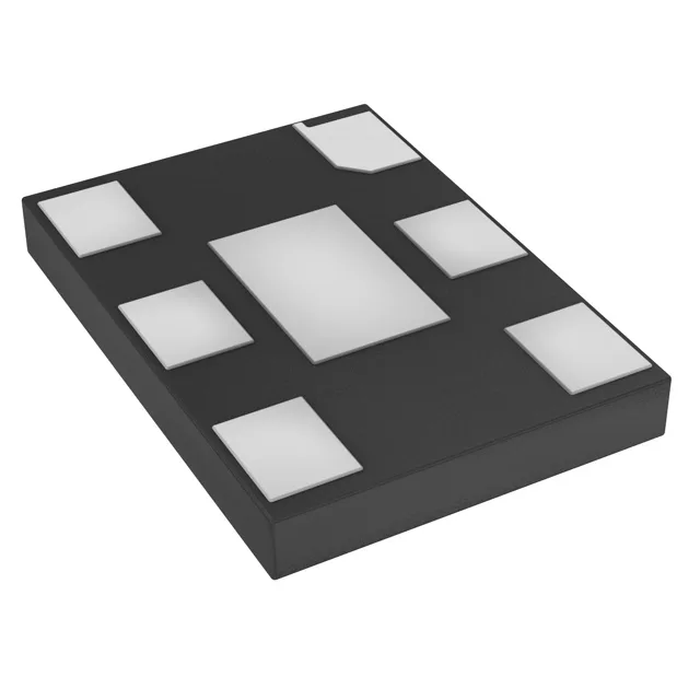
125 MHz LVDS clock for FPGA and SERDES reference
LVDS differential signalling keeps the edge jitter low over short PCB traces, which matters when the clock fans out to multiple SERDES lanes or a clock-tree buffer.
The 2.25V to 3.63V supply range covers both 2.5V and 3.3V rails without an intermediate regulator — a single rail powers the oscillator and the downstream logic.
Enable/Disable function and package footprint
Housed in a 7.00 mm × 5.00 mm 6-SMD package with an exposed pad, the footprint matches industry-standard 7×5 mm ceramic and plastic oscillators, simplifying board layout reuse.