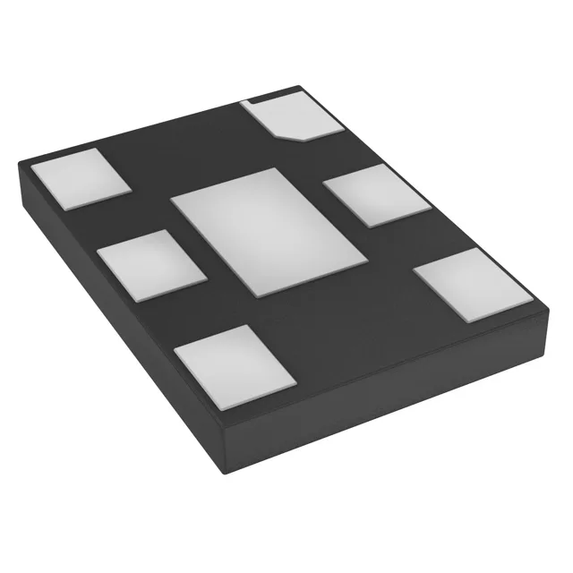
125 MHz LVDS clock source with AEC-Q100 grade
AEC-Q100 qualification and supply voltage range
It is suited for engine-control modules, ADAS sensor interfaces, and body-domain controllers that must survive under-hood thermal profiles. The supply range of 2.25 V to 3.63 V covers 2.5 V and 3.3 V rails without an external regulator, simplifying the power tree.
Housed in a 7.00 mm x 5.00 mm 6-SMD package with no lead exposed pad, the footprint matches industry-standard 7050 XO pinouts. The LVDS output requires a 100-Ω termination resistor across the differential pair at the receiver — the trace pair should be length-matched and impedance-controlled to preserve the 125 MHz edge integrity.