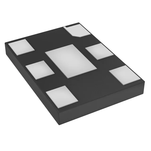
Microchip Technology DSC1121AI2-081.0000 — Crystals & Oscillators

DSC1121AI2-081.0000 MEMS XO 81 MHz CMOS ±25 ppm -40°C to

MPNDSC1121AI2-081.0000
Active

Microchip Technology DSC1121 series, XO (Standard) MEMS oscillator, 81 MHz CMOS output, ±25 ppm stability, 2.25V~3.6V supply, -40°C~85°C, 6-VDFN exposed pad package

Sourced new & surplus through independent channelsAuthenticity-screened · ESD-safe packingListing updated Aug 2026

Specifications

DSC1121AI2-081.0000 specifications
ParameterValue
TypeXO (Standard)
SeriesDSC1121
MountingSurface Mount
Voltage2.25V ~ 3.6V
Current - supply35mA
Current - supply (Disable)22mA
Frequency81 MHz
Frequency stability±25ppm
Operating temperature-40°C~85°C
Size (Dimension)0.276\" L x 0.197\" W (7.00mm x 5.00mm)
Height - seated0.035\" (0.90mm)
OutputCMOS
PackageTube
FunctionEnable/Disable
Base resonatorMEMS
Case6-VDFN Exposed Pad

Product details

MEMS resonator replaces quartz — 81 MHz fixed-frequency XO

The MEMS resonator is sealed in a silicon package, which eliminates the startup reliability issues that can plague quartz crystals in high-vibration or cold-start environments.

Supply flexibility and enable/disable function

The 6-VDFN exposed pad package (7.00mm x 5.00mm, 0.90mm seated height) requires a thermal pad on the PCB to keep the junction temperature within the industrial band.

Active lifecycle — sourced per RFQ

Product status is Active per Microchip Technology. No last-time-buy window or successor has been announced.

Frequently asked questions

Is DSC1121AI2-081.0000 compatible with 3.3V and 2.5V supplies?

Yes. The supply voltage range is 2.25V to 3.6V, so it operates on both 3.3V and 2.5V rails without a separate regulator. The ±25 ppm stability is maintained across the full voltage range.

Can DSC1121AI2 replace a standard quartz oscillator?

Functionally yes — it is a drop-in XO replacement with CMOS output. The key difference is the MEMS resonator: no quartz blank, no external load capacitors, and better shock/vibration tolerance. The package is a 6-VDFN with exposed pad, so the PCB footprint must match the 7.00mm x 5.00mm land pattern.