That frequency is a standard telecom/data-com rate used in 1 GbE, SONET/SDH, and PCIe Gen 1/2 reference clocks, so it drops straight into the clock tree without a PLL multiplier.
Supply flexibility and output control
The enable/disable pin tri-states the output — useful for power-down sequencing or in-circuit test isolation without cycling the supply. For a 155.52 MHz clock, that translates to a maximum frequency error of about ±7.8 kHz — tight enough for most 1 GbE and PCIe Gen 1/2 links without a separate VCXO or PLL cleanup stage.
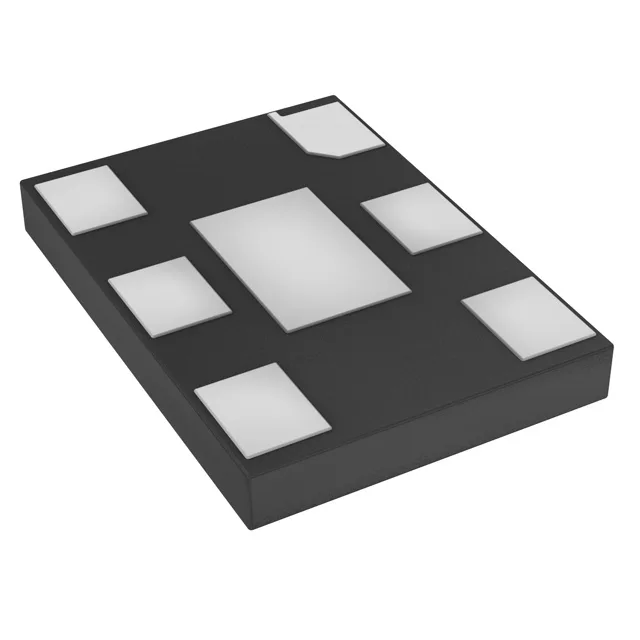
The 6-SMD package with no-lead exposed pad measures 7.00 mm × 5.00 mm with a seated height of 0.90 mm. Reworking this package under hot air is straightforward: the pad pitch is wide enough that a standard fine-tip nozzle clears the adjacent components. The orientation mark is on the top surface — confirm pin 1 location before placement, because the exposed pad is symmetric and a 180° rotation will short the output to ground.