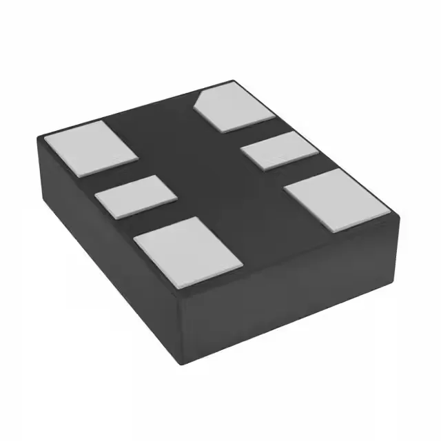
316 MHz HCSL oscillator for high-speed serial clocks
The HCSL swing and common-mode voltage are specified for direct coupling to a downstream PLL without level translation, saving two resistors per trace compared to an LVDS clock. Supply voltage spans 2.25V to 3.6V, covering the 2.5V and 3.3V rails common in FPGA and switch ASIC clock trees. The wide input range also absorbs a poorly regulated 3.3V rail that dips under load without losing lock.
Industrial temperature band and MEMS reliability
Maximum supply current is 42 mA at 316 MHz — the HCSL output stage draws more than a CMOS oscillator at the same frequency, but the differential signal integrity saves power at the receiver by eliminating the common-mode termination resistors a single-ended clock would need.
Standby power-down function
This is useful for systems that gate the clock to an idle PCIe lane or put the FPGA core into a low-power state while retaining the oscillator's startup time budget.
6-VDFN package and board layout
Housed in a 6-VDFN package measuring 3.20 mm x 2.50 mm with a seated height of 0.90 mm — a compact footprint that fits under a mezzanine card or on a tight FPGA-side clock fan-out.