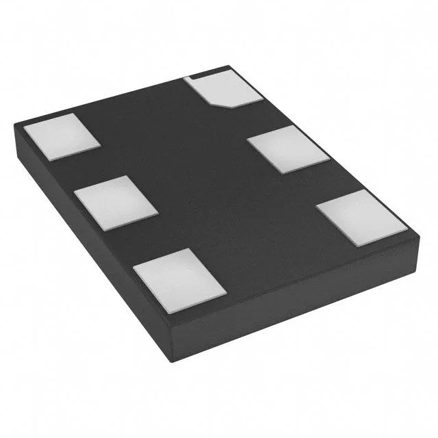
400 MHz LVDS MEMS clock source for SERDES and FPGA reference designs
The DSC1103NI1-400.0000 is a 400 MHz XO (Standard) with LVDS output, built around a MEMS resonator rather than a quartz crystal — the MEMS die is sealed at wafer level, so the part holds ±50 ppm frequency stability across -40°C to 85°C without the ageing drift of a quartz blank. At 400 MHz LVDS, this oscillator serves as the reference clock for 10GbE PHYs, FPGA transceivers, and SERDES devices that need a low-jitter differential input — the LVDS output swings 350 mV typical into a 100-Ω termination, which most high-speed SERDES blocks accept directly.
The 2.25V to 3.63V supply range means the oscillator can run from a 2.5V or 3.3V rail without an extra LDO — useful when the FPGA bank voltage is 2.5V and the rest of the board is 3.3V, because the same part number covers both builds.
6-SMD no-lead package and board integration
Housed in a 7.00 mm × 5.00 mm 6-SMD no-lead package with a seated height of 0.90 mm — the footprint matches industry-standard 7×5 mm oscillator pads, so it drops onto existing layouts without a board spin.