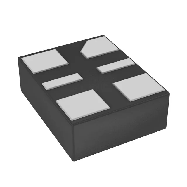
50 MHz LVDS clock source with MEMS reliability
Output is LVDS, which means the differential pair delivers clean edges into 100-ohm terminated traces — a natural fit for clocking SERDES, FPGAs, or high-speed ADCs where single-ended CMOS would pick up noise.
Industrial temperature grade and standby power savings
Supply range and package footprint
Supply voltage spans 2.25 V to 3.63 V, covering both 2.5 V and 3.3 V rails without a separate regulator — one BOM line serves multiple board variants. The 6-SMD, No Lead package measures 2.50 mm x 2.00 mm with a seated height of 0.90 mm — it fits the same footprint as many quartz oscillators, so a board designed for a 2.5 x 2.0 mm XO can take this MEMS part without a layout change.
No last-time-buy or end-of-life notice has been issued, so procurement can commit to the BOM line without a short-window risk.