180 MHz LVDS clock for high-speed serial links
The 180 MHz carrier is a natural fit for 1 Gigabit Ethernet (125 MHz reference) and PCIe Gen1/2 reference clocks, where LVDS common-mode rejection keeps the clock clean across a noisy backplane.
Standby power-down for system-level gating
The disable pin is active-low; pulling it low stops the output and puts the MEMS resonator into a low-power idle state. Wake-up time from standby is typically under 10 ms — budget this into the power-up sequence if the clock must be stable before the FPGA or SoC de-asserts its reset.
Wide supply range simplifies rail selection
The 2.25 V to 3.63 V supply range covers 2.5 V and 3.3 V rails without an external LDO — the oscillator runs directly off the FPGA or PHY bank voltage, saving a regulator and a decoupling cap.
Package and footprint for space-constrained boards
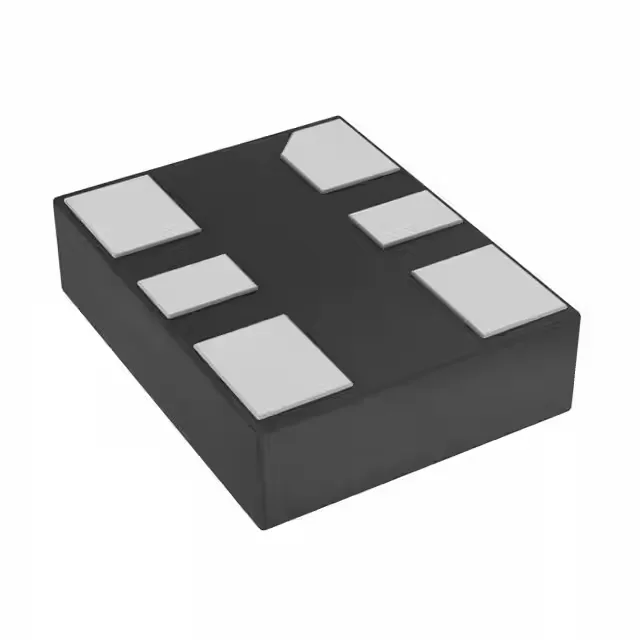
Housed in a 6-SMD, no-lead package measuring 3.20 mm x 2.50 mm with a seated height of 0.90 mm — the 2.5 mm width allows routing between 1.27 mm-pitch BGA balls on a single signal layer.