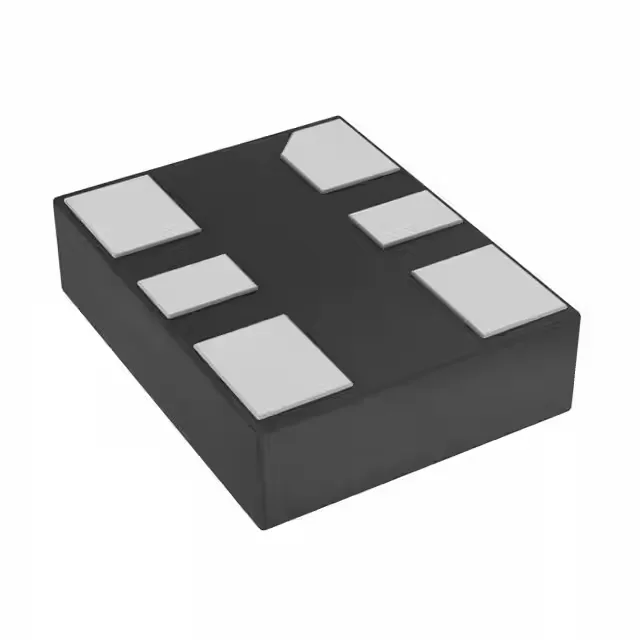
200 MHz LVDS clock source for high-speed timing
Standby power-down and wide supply tolerance
The supply voltage range spans 2.25 V to 3.63 V, so the same BOM line serves both a 2.5 V FPGA bank and a 3.3 V clock fan-out buffer without a dedicated regulator.
The 6-SMD no-lead package (3.20 mm x 2.50 mm) is a common footprint shared with other DSC1103 frequency variants, so a single PCB layout can be populated with different frequencies from the same series.