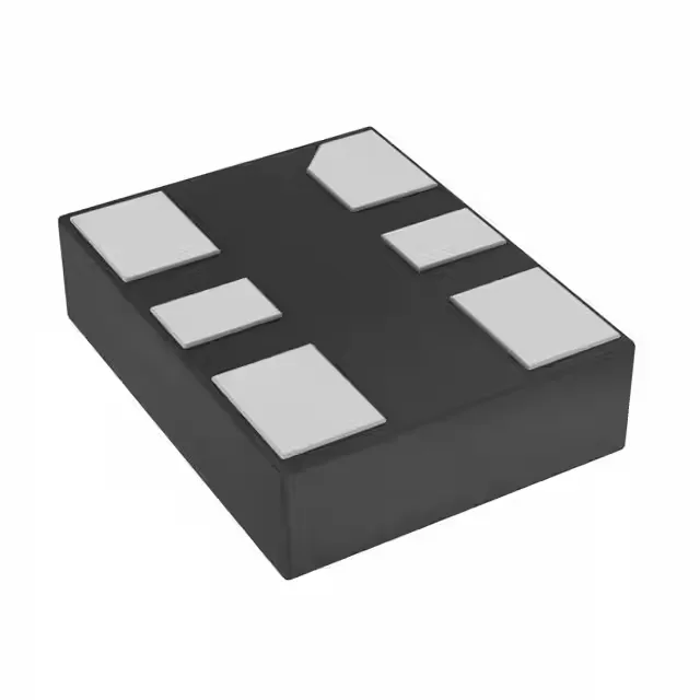
125 MHz LVDS MEMS oscillator — ±25 ppm over industrial temperature
The LVDS output provides a low-jitter, differential signal that drives long PCB traces or twisted-pair cables without the common-mode noise coupling that single-ended clocks suffer in motor-drive or switching-regulator environments.
Supply range and power-down mode
The 2.25V to 3.63V supply range lets the oscillator share a 2.5V or 3.3V rail without an extra regulator — a single 3.3V rail feeding the FPGA bank and the reference clock keeps the BOM count low.
Package, footprint, and mounting
The 6-SMD, No Lead package measures 3.20mm x 2.50mm with a seated height of 0.90 mm — the 0.126" x 0.098" footprint matches the industry-standard 3.2x2.5 mm oscillator land pattern, so the PCB layout is compatible with quartz oscillators of the same size. Surface-mount reflow follows standard JEDEC profiles; the MEMS die is hermetically sealed at the wafer level, so no moisture sensitivity level (MSL) derating is needed beyond the standard floor life.
The MEMS oscillator family has a long manufacturing runway — Microchip has not announced a successor or last-time-buy window for this DSC1103 series variant.