The LVDS signalling gives it the edge for differential clock distribution over twisted-pair or controlled-impedance traces — think gigabit Ethernet PHY reference clocks, FPGA transceiver reference clocks, or high-speed ADC/DAC sample clocks where common-mode noise rejection matters.
Runs from a 2.25V to 3.63V supply — yes, it works at 3.3V, and also at 2.5V for low-voltage logic domains. Maximum supply current is 32 mA at 125 MHz, so budget about 100 mW on the 3.3V rail.
That covers most indoor electronics, office equipment, and controlled-environment industrial gear. Not rated for -40°C cold starts or under-hood automotive use; if your design lives in a heated rack or a climate-controlled lab, this is fine.
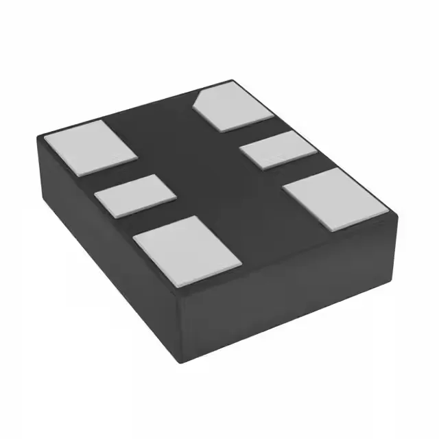
Housed in a 6-SMD, no-lead package measuring 3.20 mm x 2.50 mm with a seated height of 0.90 mm. No exposed thermal pad; decouple the supply pin with a 0.1 µF ceramic as close as possible to the package.
This is a current production part suitable for new designs. No pin-compatible second source confirmed from other manufacturers, but the DSC1103 series includes multiple frequency and stability variants if your clock tree changes.