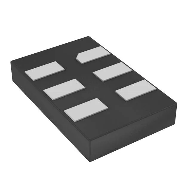
200 MHz LVDS clock source — active production
The LVDS output delivers a low-jitter differential pair suited for high-speed serial links, FPGA reference clocks, and SERDES applications where single-ended noise margins are tight. Supply voltage spans 2.25 V to 3.63 V, covering common 2.5 V and 3.3 V rails without an external regulator. The wide input range means the same BOM line can serve boards with different core voltages — useful when a design is reused across product variants. For a system that sleeps between bursts — say a wireless sensor node or a remote data logger — this keeps the clock's quiescent draw below the MCU's deep-sleep budget.
Industrial temperature range and package fit
The 6-SMD no-lead package (5.00 mm × 3.20 mm, 0.90 mm seated height) is a standard footprint shared by many MEMS and quartz oscillators. The 0.197" × 0.126" land pattern matches the common 5×3.2 mm oscillator pad layout — a drop-in replacement for quartz parts in the same form factor, provided the supply and output type match.