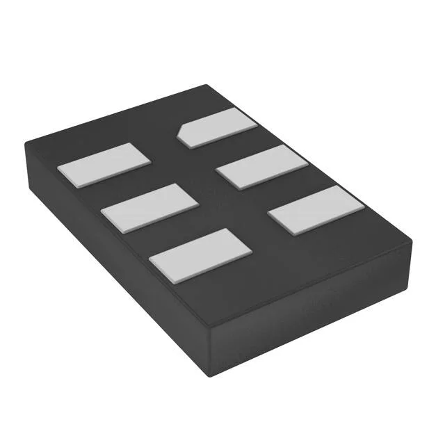
135 MHz LVDS clock source with standby
LVDS differential signaling keeps noise coupling low on the board and supports longer trace runs than single-ended clocks — useful when the FPGA or ASIC sits more than a few centimetres from the oscillator. That margin covers most 1 GbE, SATA, and PCIe reference clock requirements without needing a temperature-compensated part.
Supply voltage range is 2.25 V to 3.63 V, covering both 2.5 V and 3.3 V rails.
6-SMD, No Lead package measuring 5.00 mm x 3.20 mm with a seated height of 0.90 mm.
Product status is Active per Microchip. No stock-holding claim; sourced through independent distribution channels.