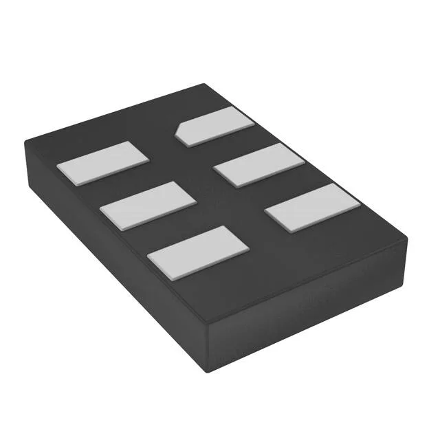
75 MHz LVDS clock source with MEMS reliability
It can be designed into new builds today without obsolescence risk. Availability confirmed at RFQ.
6-SMD no-lead — layout considerations
Housed in a 5.00 mm × 3.20 mm, 6-SMD no-lead package with a seated height of 0.90 mm. The no-lead footprint means the PCB land pattern uses a solder-paste stencil with a 0.15–0.20 mm aperture reduction to avoid bridging on the centre pad. Standard reflow profile for JEDEC MSL-1 applies — no bake required before assembly.