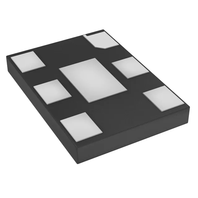
120 MHz LVDS clock source with MEMS reliability
The LVDS signal pair delivers low-jitter clocking over long PCB traces and through connectors — a typical fit for 1 Gigabit Ethernet PHYs, FPGA reference clocks, and high-speed ADC/DAC sample clocks where single-ended CMOS would pick up noise. For a 120 MHz carrier, ±10 ppm corresponds to a maximum frequency error of ±1200 Hz — tight enough to keep a 10/100/1000BASE-T Ethernet link within the ±50 ppm total tolerance budget without manual calibration.
Standby function and supply range
In a battery-powered system that gates the oscillator off between bursts, the 32 mA active current draw (max) is only present when the clock is actually needed. Supply voltage range is 2.25 V to 3.63 V, covering common 2.5 V and 3.3 V rails without an external LDO. The wide tolerance also allows the oscillator to ride through a 3.3 V rail that droops to 2.5 V under load — a common scenario in mixed-voltage FPGA banks.
The 6-SMD package (7.00 mm x 5.00 mm footprint, 0.90 mm seated height) is a standard MEMS oscillator land pattern shared with many quartz oscillators of the same size — board layout reuse is straightforward.