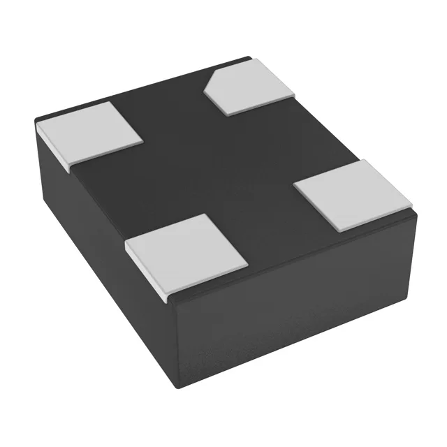
6.14 MHz MEMS XO — industrial timing with ±25 ppm hold
4-SMD no-lead footprint — reflow profile and layout
The 3.20 mm x 2.50 mm package has a 0.90 mm seated height and no exposed leads — the solder joint forms under the package terminations, so the PCB land pattern must match the recommended footprint to avoid tombstoning. Standard lead-free reflow profiles are compatible; the MEMS die and CMOS ASIC inside are rated for the same thermal exposure as a typical ceramic resonator.