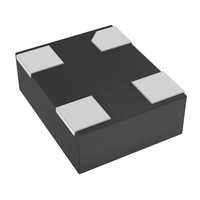
The DSC1003DL5-100.0000T carries AEC-Q100 qualification — this is the automotive IC stress qualification standard, not just an industrial-grade part dressed up for the engine bay. At 100 MHz, a 10 ppm shift is 1 kHz of deviation; the receiver PLL can track that, but a 50 ppm part would push the jitter budget.
Max supply current is 9.6 mA at 100 MHz — low enough for a sensor node or telematics module that runs on a 12 V battery through a linear regulator. Supply voltage range of 1.7 V to 3.6 V covers common 1.8 V and 3.3 V logic rails. No external level translator needed when the MCU or SoC runs at 1.8 V — the oscillator output swings CMOS directly into the clock input.
Package footprint and layout considerations
4-VDFN package measuring 2.50 mm x 2.00 mm with a seated height of 0.90 mm — this fits under a shield can or a low-profile enclosure. The 4-pin land pattern has a centre pad; ensure the PCB has a solid via-stitched ground pad under the package for thermal and electrical return.