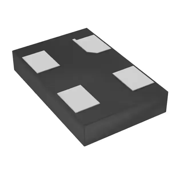
The DSC1001BI2-024.5760 is a MEMS-based XO (Standard) from Microchip's DSC1001 series, delivering a 24.576 MHz CMOS output at ±25 ppm stability over -40 to 85 °C. That ±25 ppm is tight enough for 48 kHz audio clock trees and CAN-FD bit timing without a TCXO, and the -40 to 85 °C range covers the cabin and most under-hood locations — provided the ambient stays below the 85 °C ceiling. For a Tier-1 ECU program, this is the PPAP-ready timing source — no separate qualification report needed from the supplier.
Standby function saves 6.3 mA per oscillator
In an ECU that sleeps 90 % of the time, that difference — 6.285 mA per oscillator — extends the module's quiescent budget significantly. The output goes high-impedance in standby, so the downstream clock receiver sees a clean stop without runt pulses.
1.8–3.3 V supply, single BOM line
The 1.8 V to 3.3 V supply range lets this XO serve 1.8 V MCU cores, 2.5 V FPGA banks, and 3.3 V peripheral buses from the same order code. No separate supply rail or level translator is needed — just a single 100 nF decoupling cap within 2 mm of the Vdd pin, per the MEMS oscillator layout best practice.
Housed in a 4-SMD, No Lead package measuring 5.00 mm × 3.20 mm with a seated height of 0.90 mm. The no-lead land pattern is a standard 4-pad footprint — the two centre pads are the corner ground and the no-connect; the outer two are Vdd and Output. Surface-mount reflow per JEDEC J-STD-020; MSL rating is not in evidence, but the MEMS die is inherently moisture-insensitive.