Operating from 1.8 V to 3.3 V, this oscillator spans the common digital supply rails — a single BOM line covers 1.8 V FPGA banks, 2.5 V SERDES PLLs, and 3.3 V MCU clock inputs without a separate level translator.
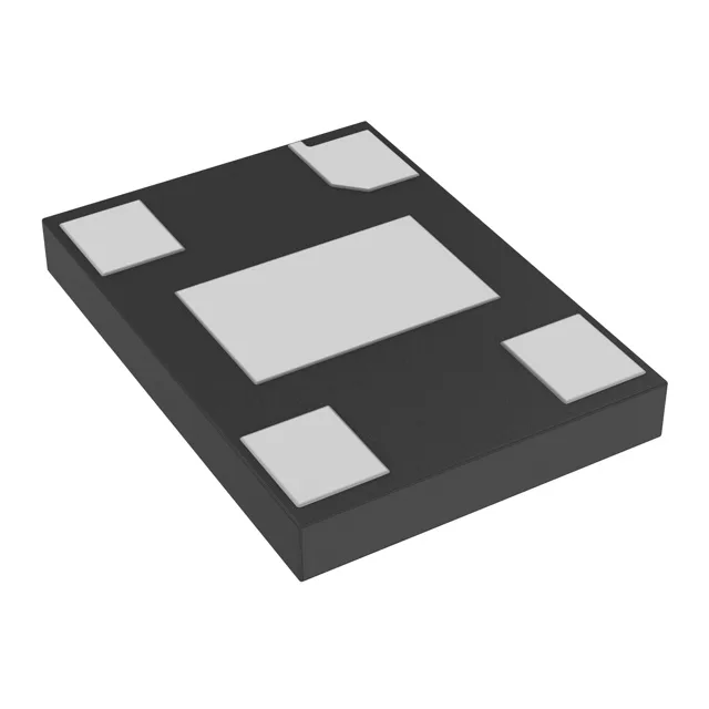
Housed in a 4-SMD, no-lead exposed pad package measuring 7.00 mm × 5.00 mm with a seated height of 0.90 mm, the footprint matches the industry-standard 7×5 mm oscillator land pattern — a direct solder-paste stencil replacement for quartz oscillators in the same outline. Surface-mount assembly on standard PCB with no special via-in-pad requirements; the exposed pad provides a low-thermal-resistance path to the board ground plane, though the 8.7 mA draw rarely demands it.