10 ns propagation delay — what it buys on the bus
The ATF16V8B-10JI is an electrically erasable programmable logic device (EE PLD) from Microchip's 16V8 family, offering a 10 ns propagation delay from input to combinatorial output. That 10 ns window sets the timing budget for address decoding, state-machine transitions, or bus-interface gating in a 5V system — if the downstream register setup time plus trace delay exceeds 10 ns, the path misses the window. With 8 macrocells, this part handles small-scale glue logic: think chip-select generation for a handful of memory-mapped peripherals or a simple 4-state sequencer.
5V-only supply — legacy rail commitment
This PLD runs on a single 5V supply with no on-chip regulator for lower-voltage operation. If your board has migrated to a 3.3V core rail, the ATF16V8B-10JI needs a separate 5V plane and level translators on every I/O crossing domains — a non-trivial board-spin cost. The 5V input threshold also means the part cannot directly sense 1.8V or 2.5V logic levels without external biasing.
20-PLCC footprint — rework and layout notes
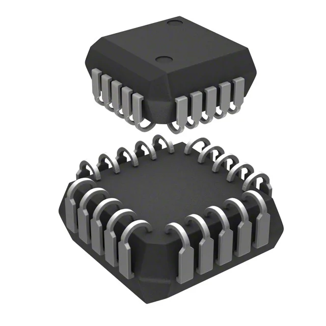
The 20-PLCC (9x9 mm) J-Lead package is a surface-mount legacy footprint. Unlike gull-wing leads, the J-bend hides the solder joint under the package body, so visual inspection after reflow is limited — X-ray or a boundary-scan test is the reliable verification method. For rework, a hot-air nozzle that matches the PLCC body profile is needed; the J-leads reflow at a slightly higher thermal mass than a standard SOIC, so the preheat zone should be extended by 10–15 seconds to avoid cold joints on the centre pads.
For a BOM line that must stay with the 20-PLCC footprint and 5V supply, the only channel is independent distribution sourcing surplus or last-time-buy inventory.